
silicon
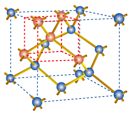
In the basic unit of a crystalline silicon solid, a silicon atom shares each of its four valence electrons with each of four neighboring atoms.
Silicon (si) is a chemical element with the atomic number 14 that is semimetallic in nature and dark gray. Silicon is the material most commonly used in semiconductor devices such as solar cells.
Silicon occurs naturally in various forms including silica (silicon dioxide) of which sand and quartz are composed. It crystallizes in the form of a face-centered cubic lattice like that of diamond. As the second most abundant element in the Earth's crust, silicon is plentifully available and has the additional advantage that its processing does not burden the environment. To be useful in semiconductor devices, silicon must be doped with impurities.
Silicon in solar (photovoltaic) devices
Silicon, which was used to make some the earliest photovoltaic (PV) devices, is still the most popular material for solar cells. Outranked only by oxygen, silicon is also the second-most abundant element in the Earth's crust. However, to be useful as a semiconductor material in solar cells, silicon must be refined to a purity of 99.9999%. In single-crystal silicon, the molecular structure – the arrangement of atoms in the material – is uniform, because the entire structure is grown from the same crystal. This uniformity is ideal for transferring electrons efficiently through the material. To make an effective PV cell, however, silicon has to be "doped" with other elements to make it n-type and p-type.
Semicrystalline silicon, in contrast, consists of several smaller crystals or grains, which introduce boundaries. These boundaries impede the flow of electrons and encourage them to recombine with holes to reduce the power output of the solar cell. However, semicrystalline silicon is much less expensive to produce than single-crystalline silicon. So researchers are working on other ways to minimize the effects of grain boundaries.
In this article, we will cover silicon solar cell materials in detail:
Single-crystal silicon
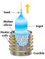 |
| The most widely used technique for making single-crystal silicon is the Czochralski process, in which a seed of single-crystal silicon contacts the top of molten silicon. As the seed is slowly raised, atoms of the molten silicon solidify in the pattern of the seed and extend the single-crystal structure |

|
| After a silicon ingot is grown, it must be sawn it into thin wafers for further processing into PV cells |
To create silicon in a single-crystal state, we must first melt high-purity silicon. We then cause it to reform or solidify very slowly in contact with a single crystal "seed." The silicon adapts to the pattern of the single-crystal seed as it cools and gradually solidifies. Not surprisingly, because we start from a seed, we say that this process is "growing" a new rod (often called a "boule") of single-crystal silicon out of molten silicon.
Several different processes can be used to grow a boule of single-crystal silicon. The most established and dependable processes are the Czochralski (Cz)method and the float-zone (FZ) technique. We also discuss "ribbon-growth" techniques.
Czochralski silicon
In the Czochralski process, a seed crystal is dipped into a crucible of molten silicon and withdrawn slowly, pulling a cylindrical single crystal as the silicon crystallizes on the seed.
Float-zone silicon
The float-zone process produces purer crystals than the Czochralski method, because they are not contaminated by the crucible used in growing Czochralski crystals. In the float-zone process, a silicon rod is set atop a seed crystal and then lowered through an electromagnetic coil. The coil's magnetic field induces an electric field in the rod, heating and melting the interface between the rod and the seed. Single-crystal silicon forms at the interface, growing upward as the coils are slowly raised.
Once the single-crystal rods are produced, by either the Cz or FZ method, they must be sliced or sawn to form thin wafers. Such sawing, however, wastes as much as 20% of the valuable silicon as sawdust, known as "kerf." The resulting thin wafers are then doped to produce the necessary electric field. They are then treated with a coating to reduce reflection, and coated with electrical contacts to form functioning PV cells.
Ribbon silicon
Although single-crystal silicon technology is well developed, the Czochralski and float-zone processes are complex and expensive (as are the ingot-casting processes discussed under multicrystalline silicon). Another group of crystal-producing processes, however, goes by the general name of "ribbon growth." These single crystals may cost less than other processes, because they form the silicon directly into thin, usable wafers of single-crystal silicon. These methods involve forming thin crystalline sheets directly, thus avoiding the slicing step required of cylindrical rods.
One "ribbon growth" technique – edge-defined film-fed growth – starts with two crystal seeds that grow and capture a sheet of material between them as they are pulled from a source of molten silicon. A frame entrains a thin sheet of material when drawn from a melt. This technique does not waste much material, but the quality of the material is not as high as Cz and FZ silicon.
Multicrystalline silicon
Multicrystalline silicon devices are generally less efficient than those of single-crystal silicon, but they can be less expensive to produce. The multicrystalline silicon can be produced in a variety of ways. The most popular commercial methods involve a casting process in which molten silicon is directly cast into a mold and allowed to solidify into an ingot. The starting material can be a refined lower-grade silicon, rather that the higher-grade semiconductor grade required for single-crystal material. The cooling rate is one factor that determines the final size of crystals in the ingot and the distribution of impurities. The mold is usually square, producing an ingot that can be cut and sliced into square cells that fit more compactly into a PV module. (Round cells have spaces between them in modules, but square cells fit together better with a minimum of wasted space).
Amorphous silicon
 |
In 1974, researchers began to realize that they could use amorphous silicon in PV devices by properly controlling the conditions under which it is deposited and by carefully modifying its composition. Today, amorphous silicon is common in solar-powered consumer devices that have low power requirements, such as wristwatches and calculators.
Amorphous silicon absorbs solar radiation 40 times more efficiently than does single-crystal silicon, so a film only about 1 micrometer – or one one-millionth of a meter – thick can absorb 90% of the usable light energy shining on it. This is one of the chief reasons that amorphous silicon could reduce the cost of photovoltaics. Other economic advantages are that it can be produced at lower temperatures and can be deposited on low-cost substrates such as plastic, glass, and metal. This makes amorphous silicon ideal for building-integrated PV products like the one shown in the photo. And these characteristics make amorphous silicon the leading thin-film PV material.
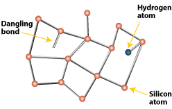
Amorphous silicon's random structural characteristics cause deviations like "dangling bonds." Dangling bonds provide places for electrons to recombine with holes, but they may be neutralized somewhat with hydrogen.
A closer look
Amorphous silicon does not have the structural uniformity of single- or multicrystalline silicon. Small deviations in this material result in defects such as "dangling bonds," where atoms lack a neighbor to which they can bond. These defects provide places for electrons to recombine with holes, rather than contributing to the electrical circuit. Ordinarily, this kind of material would be unacceptable for electronic devices, because defects limit the flow of current. But amorphous silicon can be deposited so that it contains a small amount of hydrogen, in a process called "hydrogenation." The result is that the hydrogen atoms combine chemically with many of the dangling bonds, essentially removing them and permitting electrons to move through the material.
Staebler-Wronski effect
Instability is the greatest stumbling block for amorphous silicon. These cells experience the Staebler-Wronski effect, where their electrical output decreases over a period of time when first exposed to sunlight. Eventually, however, the electrical output stabilizes. This effect can result in up to a 20% loss in output before the material stabilizes. Exactly why this effect occurs is not fully understood, but part of the reason is likely related to the amorphous hydrogenated nature of the material. One way to mitigate – though not eliminate – this effect is to make amorphous silicon cells that have a multijunction design (discussed in another section).
Cell design
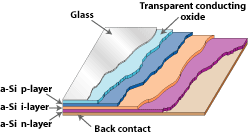 |
| A typical amorphous silicon cell employs a p-i-n
design, in which an intrinsic layer (i-layer) is sandwiched between
a p-layer and an n-layer
|
Because of amorphous silicon's unique properties, solar cells are designed to have an ultrathin (0.008 micrometer) p-type top layer, a thicker (0.5 to 1 micrometer) intrinsic middle layer, and a very thin (0.02 micrometer) n-type bottom layer. This design is called a "p-i-n" structure, being named for the types of the three layers. The top layer is made so thin and relatively transparent that most light passes right through it, to generate free electrons in the intrinsic layer. The p- and n-layers produced by doping the amorphous silicon create an electric field across the entire intrinsic region, thus inducing electron movement in that i-layer.